1480 :)...quanto arriverà in overclock?
1800:lol:
- - - Updated - - -
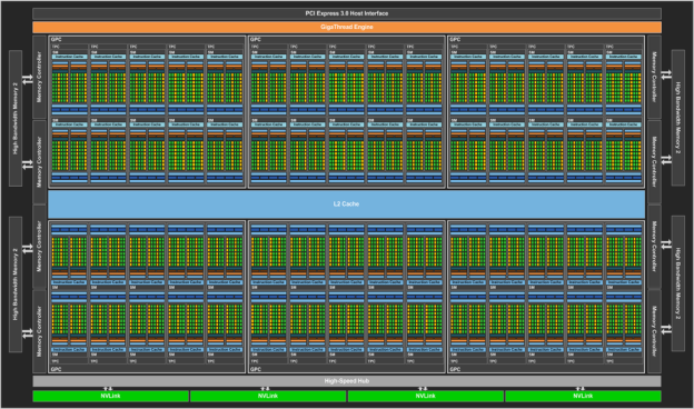
Certo che 610mm2 è la gpu più grande mai prodotta.... batte l'enorme gm200 (601mm2)
mamma mia sono già innamorato, è immensa
- - - Updated - - -
comunque ragazzi 3584 cc fp32
quindi i 4096 cc di gp104 erano completamente fasulli
[TABLE="width: 1"]
[TR]
[TD]
Tesla Products[/TD]
[TD="width: 117"]
Tesla K40[/TD]
[TD="width: 123"]
Tesla M40[/TD]
[TD="width: 116"]
Tesla P100[/TD]
[/TR]
[TR]
[TD="width: 122"]
GPU[/TD]
[TD="width: 117"]GK110 (Kepler)[/TD]
[TD="width: 123"]GM200 (Maxwell)[/TD]
[TD="width: 116"]GP100 (Pascal)[/TD]
[/TR]
[TR]
[TD="width: 122"]
SMs[/TD]
[TD="width: 117"]15[/TD]
[TD="width: 123"]24[/TD]
[TD="width: 116"]56[/TD]
[/TR]
[TR]
[TD="width: 122"]
TPCs[/TD]
[TD="width: 117"]15[/TD]
[TD="width: 123"]24[/TD]
[TD="width: 116"]28[/TD]
[/TR]
[TR]
[TD="width: 122"]
FP32 CUDA Cores / SM[/TD]
[TD="width: 117"]192[/TD]
[TD="width: 123"]128[/TD]
[TD="width: 116"]64[/TD]
[/TR]
[TR]
[TD="width: 122"]
FP32 CUDA Cores / GPU[/TD]
[TD="width: 117"]2880[/TD]
[TD="width: 123"]3072[/TD]
[TD="width: 116"]3584[/TD]
[/TR]
[TR]
[TD="width: 122"]
FP64 CUDA Cores / SM[/TD]
[TD="width: 117"]64[/TD]
[TD="width: 123"]4[/TD]
[TD="width: 116"]32[/TD]
[/TR]
[TR]
[TD="width: 122"]
FP64 CUDA Cores / GPU[/TD]
[TD="width: 117"]960[/TD]
[TD="width: 123"]96[/TD]
[TD="width: 116"]1792[/TD]
[/TR]
[TR]
[TD="width: 122"]
Base Clock[/TD]
[TD="width: 117"]745 MHz[/TD]
[TD="width: 123"]948 MHz[/TD]
[TD="width: 116"]1328 MHz[/TD]
[/TR]
[TR]
[TD="width: 122"]
GPU Boost Clock[/TD]
[TD="width: 117"]810/875 MHz[/TD]
[TD="width: 123"] 1114 MHz[/TD]
[TD="width: 116"]1480 MHz[/TD]
[/TR]
[TR]
[TD="width: 122"]
FP64 GFLOPs[/TD]
[TD="width: 117"]1680[/TD]
[TD="width: 123"]213[/TD]
[TD="width: 116"]5304
[1][/TD]
[/TR]
[TR]
[TD="width: 122"]
Texture Units[/TD]
[TD="width: 117"]240[/TD]
[TD="width: 123"]192[/TD]
[TD="width: 116"]224[/TD]
[/TR]
[TR]
[TD="width: 122"]
Memory Interface[/TD]
[TD="width: 117"]384-bit GDDR5[/TD]
[TD="width: 123"]384-bit GDDR5[/TD]
[TD="width: 116"]4096-bit HBM2[/TD]
[/TR]
[TR]
[TD="width: 122"]
Memory Size[/TD]
[TD="width: 117"]Up to 12 GB[/TD]
[TD="width: 123"]Up to 24 GB[/TD]
[TD="width: 116"]16 GB[/TD]
[/TR]
[TR]
[TD="width: 122"]
L2 Cache Size[/TD]
[TD="width: 117"]1536 KB[/TD]
[TD="width: 123"]3072 KB[/TD]
[TD="width: 116"]4096 KB[/TD]
[/TR]
[TR]
[TD="width: 122"]
Register File Size / SM[/TD]
[TD="width: 117"]256 KB[/TD]
[TD="width: 123"]256 KB[/TD]
[TD="width: 116"]256 KB[/TD]
[/TR]
[TR]
[TD="width: 122"]
Register File Size / GPU[/TD]
[TD="width: 117"]3840 KB[/TD]
[TD="width: 123"]6144 KB[/TD]
[TD="width: 116"]14336 KB[/TD]
[/TR]
[TR]
[TD="width: 122"]
TDP[/TD]
[TD="width: 117"]235 Watts[/TD]
[TD="width: 123"]250 Watts[/TD]
[TD="width: 116"]300 Watts[/TD]
[/TR]
[TR]
[TD="width: 122"]
Transistors[/TD]
[TD="width: 117"]7.1 billion[/TD]
[TD="width: 123"]8 billion[/TD]
[TD="width: 116"]15.3 billion[/TD]
[/TR]
[TR]
[TD="width: 122"]
GPU Die Size[/TD]
[TD="width: 117"]551 mm²[/TD]
[TD="width: 123"]601 mm²[/TD]
[TD="width: 116"]610 mm²[/TD]
[/TR]
[TR]
[TD="width: 122"]
Manufacturing Process[/TD]
[TD="width: 117"]28-nm[/TD]
[TD="width: 123"]28-nm[/TD]
[TD="width: 116"]16-nm[/TD]
[/TR]
[/TABLE]