DOMANDA SSD?
- Autore discussione toni1705
- Data d'inizio
Stai usando un browser non aggiornato. Potresti non visualizzare correttamente questo o altri siti web.
Dovreste aggiornare o usare un browser alternativo.
Dovreste aggiornare o usare un browser alternativo.
riccarock
Utente Èlite
- 7,970
- 2,080
- CPU
- Amd Ryzen 3700x
- Dissipatore
- Noctua NH-D15
- Scheda Madre
- Asus Rog Strix X570 F-Gaming
- HDD
- Nvme WD SN850 Black 500Gb,Kingston Renegade 2TB,Toshiba P300 3Tb,WD Red Plus 4Tb,2 Toshiba MG08 16Tb
- RAM
- Corsair Vengeance 2x8Gb 3200Mhz Cl16
- GPU
- Asus Tuf OC 3060Ti
- Audio
- Edifier 1280DBs
- Monitor
- Asus Tuf Gaming VG279QM
- PSU
- Corsair RMX 750w Shift
- Case
- Fractal Design Define R6
- Periferiche
- Tastiera Custom
- Net
- Tim Fibra 1000
- OS
- Windows 10 Pro
A me fa paura quel hdd Maxtor nn ne vedevo uno da 10 anni quasi
Metti la configurazione d tuo pc
E fossi in te cambierei anche quel HDD
Inviato dal mio MI 9 utilizzando Tapatalk
Metti la configurazione d tuo pc
E fossi in te cambierei anche quel HDD
Inviato dal mio MI 9 utilizzando Tapatalk
Che tipo di SSD per il mio pc?
vorrei compraro su Amazon, ma ho paura di sbagliare...
Potresti darmi consigli
Ciao! Guarda, dalle specifiche si vede che hai un attacco SATA II , quindi il PC è sicuramente datato, minimo sarà del 2012 circa...! Io ti suggerirei di metterci Questo SSD che è più che sufficiente ed è il massimo che puoi fare! Ovviamente non funzionerà alla massima velocità consentita (SATA III) ma va bene comunque...
che programma devo usare per la configurazione?A me fa paura quel hdd Maxtor nn ne vedevo uno da 10 anni quasi
Metti la configurazione d tuo pc
E fossi in te cambierei anche quel HDD
Inviato dal mio MI 9 utilizzando Tapatalk
si il pc è antichissimo ahahahaCiao! Guarda, dalle specifiche si vede che hai un attacco SATA II , quindi il PC è sicuramente datato, minimo sarà del 2012 circa...! Io ti suggerirei di metterci Questo SSD che è più che sufficiente ed è il massimo che puoi fare! Ovviamente non funzionerà alla massima velocità consentita (SATA III) ma va bene comunque...
avevo visto anche una cosa Simile Questo.. il prezzo è quello .. qual'è mi consiglieresti? (dovrei utilizzare un riduttore? (stiamo parlando di un pc fisso)
che programma devo usare per la configurazione?
si il pc è antichissimo ahahaha
avevo visto anche una cosa Simile Questo.. il prezzo è quello .. qual'è mi consiglieresti?
Ciao! No non c'è da mettere nessun adattatore! l'attacco sata è compatibile!
Ho già fatto un operazione simile sul notebook di mia mamma ed ha funzionato! L'esperienza d'uso migliora di molto!
Cmq se vai in impostazioni - sistema di windows 10 vedi le caratteristiche principali del PC
altrimenti se vuoi più specifiche puoi scaricare CPU_Z oppure HW info....
Post unito automaticamente:
avevo visto anche una cosa Simile Questo.. il prezzo è quello .. qual'è mi consiglieresti? (dovrei utilizzare un riduttore? (stiamo parlando di un pc fisso)
Qui sul forum si consiglia spesso l'A55 della Silicon power come SSD, proprio perchè ha un ottimo rapporto qualità /prezzo!
quel Samsung 860 EVO, te lo consiglio solo, se lo prendi in ottica di recuperarlo per una nuova build!
Altrimenti è solo che sprecato, perchè con l'attacco SATA II non sfrutti la velocità che ti darebbe quel SSD...!
PS. Non ci hai ancora detto che configurazione ha il tuo PC...
Ultima modifica:
riccarock
Utente Èlite
- 7,970
- 2,080
- CPU
- Amd Ryzen 3700x
- Dissipatore
- Noctua NH-D15
- Scheda Madre
- Asus Rog Strix X570 F-Gaming
- HDD
- Nvme WD SN850 Black 500Gb,Kingston Renegade 2TB,Toshiba P300 3Tb,WD Red Plus 4Tb,2 Toshiba MG08 16Tb
- RAM
- Corsair Vengeance 2x8Gb 3200Mhz Cl16
- GPU
- Asus Tuf OC 3060Ti
- Audio
- Edifier 1280DBs
- Monitor
- Asus Tuf Gaming VG279QM
- PSU
- Corsair RMX 750w Shift
- Case
- Fractal Design Define R6
- Periferiche
- Tastiera Custom
- Net
- Tim Fibra 1000
- OS
- Windows 10 Pro
Usa CPU Zche programma devo usare per la configurazione?
si il pc è antichissimo ahahaha
avevo visto anche una cosa Simile Questo.. il prezzo è quello .. qual'è mi consiglieresti? (dovrei utilizzare un riduttore? (stiamo parlando di un pc fisso)
Per psu e altri componenti basta aprire la paratia laterale del pc
Inviato dal mio MI 9 utilizzando Tapatalk
eccolo :)Usa CPU Z
Per psu e altri componenti basta aprire la paratia laterale del pc
Inviato dal mio MI 9 utilizzando Tapatalk
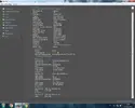
Codice:
CPU-Z TXT Report
-------------------------------------------------------------------------
Binaries
-------------------------------------------------------------------------
CPU-Z version 1.94.0.x64
Processors
-------------------------------------------------------------------------
Number of sockets 1
Number of threads 2
APICs
-------------------------------------------------------------------------
Socket 0
-- Core 0 (ID 0)
-- Thread 0 0
-- Core 1 (ID 1)
-- Thread 1 1
Timers
-------------------------------------------------------------------------
ACPI timer 3.580 MHz
Perf timer 2.922 MHz
Sys timer 1.000 KHz
Processors Information
-------------------------------------------------------------------------
Socket 1 ID = 0
Number of cores 2 (max 2)
Number of threads 2 (max 2)
Manufacturer GenuineIntel
Name Intel Core 2 Duo E6850
Codename Conroe
Specification Intel(R) Core(TM)2 Duo CPU E6850 @ 3.00GHz
Package (platform ID) Socket 775 LGA (0x0)
CPUID 6.F.B
Extended CPUID 6.F
Core Stepping G0
Technology 65 nm
Core Speed 1992.4 MHz
Multiplier x Bus Speed 6.0 x 332.1 MHz
Base frequency (cores) 332.1 MHz
Base frequency (ext.) 332.1 MHz
Rated Bus speed 1328.3 MHz
Stock frequency 3000 MHz
Instructions sets MMX, SSE, SSE2, SSE3, SSSE3, EM64T, VT-x
Microcode Revision 0xB6
L1 Data cache 2 x 32 KBytes, 8-way set associative, 64-byte line size
L1 Instruction cache 2 x 32 KBytes, 8-way set associative, 64-byte line size
L2 cache 4096 KBytes, 16-way set associative, 64-byte line size
Max CPUID level 0000000Ah
Max CPUID ext. level 80000008h
Cache descriptor Level 1, D, 32 KB, 1 thread(s)
Cache descriptor Level 1, I, 32 KB, 1 thread(s)
Cache descriptor Level 2, U, 4 MB, 2 thread(s)
FID/VID Control yes
FID range 6.0x - 9.0x
Max VID 1.350 V
Temperature 0 65 degC (149 degF) (Core #0)
Temperature 1 65 degC (149 degF) (Core #1)
Clock Speed 0 1992.45 MHz (Core #0)
Clock Speed 1 2988.67 MHz (Core #1)
Core 0 max ratio (effective) 9.0
Core 1 max ratio (effective) 9.0
Thread dumps
-------------------------------------------------------------------------
CPU Thread 0
APIC ID 0
Topology Processor ID 0, Core ID 0, Thread ID 0
CPUID
0x00000000 0x0000000A 0x756E6547 0x6C65746E 0x49656E69
0x00000001 0x000006FB 0x00020800 0x0000E3FD 0xBFEBFBFF
0x00000002 0x05B0B101 0x005657F0 0x00000000 0x2CB43049
0x00000003 0x00000000 0x00000000 0x00000000 0x00000000
0x00000004 0x04000121 0x01C0003F 0x0000003F 0x00000001
0x00000004 0x04000122 0x01C0003F 0x0000003F 0x00000001
0x00000004 0x04004143 0x03C0003F 0x00000FFF 0x00000001
0x00000005 0x00000040 0x00000040 0x00000003 0x00000220
0x00000006 0x00000001 0x00000002 0x00000001 0x00000000
0x00000007 0x00000000 0x00000000 0x00000000 0x00000000
0x00000008 0x00000400 0x00000000 0x00000000 0x00000000
0x00000009 0x00000000 0x00000000 0x00000000 0x00000000
0x0000000A 0x07280202 0x00000000 0x00000000 0x00000503
0x80000000 0x80000008 0x00000000 0x00000000 0x00000000
0x80000001 0x00000000 0x00000000 0x00000001 0x20100800
0x80000002 0x65746E49 0x2952286C 0x726F4320 0x4D542865
0x80000003 0x44203229 0x43206F75 0x20205550 0x45202020
0x80000004 0x30353836 0x20402020 0x30302E33 0x007A4847
0x80000005 0x00000000 0x00000000 0x00000000 0x00000000
0x80000006 0x00000000 0x00000000 0x10008040 0x00000000
0x80000007 0x00000000 0x00000000 0x00000000 0x00000000
0x80000008 0x00003024 0x00000000 0x00000000 0x00000000
MSR 0x0000001B 0x00000000 0xFEE00900
MSR 0x0000003A 0x00000000 0x00000001
MSR 0x00000017 0x00000000 0x8800892A
MSR 0x0000003F 0x00000000 0x000000EA
MSR 0x000000CE 0x001D092A 0x7F7F071A
MSR 0x000001A0 0x00000040 0x62862089
MSR 0x000000EE 0xA8000000 0xC37D5300
MSR 0x0000011E 0x00000000 0xBE702109
MSR 0x000000CD 0x00000000 0x00000804
MSR 0x0000019C 0x00000000 0x881D0000
MSR 0x00000198 0x092A092A 0x0600092A
MSR 0x00000199 0x00000000 0x0000092A
CPU Thread 1
APIC ID 1
Topology Processor ID 0, Core ID 1, Thread ID 0
CPUID
0x00000000 0x0000000A 0x756E6547 0x6C65746E 0x49656E69
0x00000001 0x000006FB 0x01020800 0x0000E3FD 0xBFEBFBFF
0x00000002 0x05B0B101 0x005657F0 0x00000000 0x2CB43049
0x00000003 0x00000000 0x00000000 0x00000000 0x00000000
0x00000004 0x04000121 0x01C0003F 0x0000003F 0x00000001
0x00000004 0x04000122 0x01C0003F 0x0000003F 0x00000001
0x00000004 0x04004143 0x03C0003F 0x00000FFF 0x00000001
0x00000005 0x00000040 0x00000040 0x00000003 0x00000220
0x00000006 0x00000001 0x00000002 0x00000001 0x00000000
0x00000007 0x00000000 0x00000000 0x00000000 0x00000000
0x00000008 0x00000400 0x00000000 0x00000000 0x00000000
0x00000009 0x00000000 0x00000000 0x00000000 0x00000000
0x0000000A 0x07280202 0x00000000 0x00000000 0x00000503
0x80000000 0x80000008 0x00000000 0x00000000 0x00000000
0x80000001 0x00000000 0x00000000 0x00000001 0x20100800
0x80000002 0x65746E49 0x2952286C 0x726F4320 0x4D542865
0x80000003 0x44203229 0x43206F75 0x20205550 0x45202020
0x80000004 0x30353836 0x20402020 0x30302E33 0x007A4847
0x80000005 0x00000000 0x00000000 0x00000000 0x00000000
0x80000006 0x00000000 0x00000000 0x10008040 0x00000000
0x80000007 0x00000000 0x00000000 0x00000000 0x00000000
0x80000008 0x00003024 0x00000000 0x00000000 0x00000000
MSR 0x0000001B 0x00000000 0xFEE00800
MSR 0x0000003A 0x00000000 0x00000001
MSR 0x00000017 0x00000000 0x8800892A
MSR 0x0000003F 0x00000000 0x000000EA
MSR 0x000000CE 0x001D092A 0x7F7F071A
MSR 0x000001A0 0x00000040 0x62862089
MSR 0x000000EE 0xA8000000 0xC37D5300
MSR 0x0000011E 0x00000000 0xBE702109
MSR 0x000000CD 0x00000000 0x00000804
MSR 0x0000019C 0x00000000 0x881D0000
MSR 0x00000198 0x092A092A 0x0600092A
MSR 0x00000199 0x00000000 0x0000092A
BIOS
-------------------------------------------------------------------------
UEFI No
BIOS Vendor Phoenix Technologies, LTD
BIOS Date 04/30/08
Chipset
-------------------------------------------------------------------------
Northbridge Intel Q35 rev. A2
Southbridge Intel 82801IO (ICH9DO) rev. 02
Graphic Interface PCI-Express
PCI-E Link Width x16
PCI-E Max Link Width x16
Memory Type DDR2
Memory Size 4 GBytes
Channels Dual, (Symmetric)
Memory Frequency 399.0 MHz (5:6)
CAS# latency (CL) 6.0
RAS# to CAS# delay (tRCD) 6
RAS# Precharge (tRP) 6
Cycle Time (tRAS) 18
Row Refresh Cycle Time (tRFC) 42
Command Rate (CR) 2T
Host Bridge 0x29B0
Memory SPD
-------------------------------------------------------------------------
DIMM # 1
SMBus address 0x50
Memory type DDR2
Module format Regular UDIMM
Module Manufacturer(ID) MOSEL (40000000000000000000000000)
Size 1024 MBytes
Max bandwidth PC2-6400 (400 MHz)
Part number V916765K24QCFW-G6
Serial number E6961867
Manufacturing date Week 33/Year 08
Number of banks 4
Data width 64 bits
Correction None
Nominal Voltage 1.80 Volts
EPP no
XMP no
AMP no
JEDEC timings table CL-tRCD-tRP-tRAS-tRC @ frequency
JEDEC #1 4.0-4-4-12-16 @ 266 MHz
JEDEC #2 5.0-5-5-15-20 @ 333 MHz
JEDEC #3 6.0-6-6-18-24 @ 400 MHz
DIMM # 2
SMBus address 0x51
Memory type DDR2
Module format Regular UDIMM
Module Manufacturer(ID) MOSEL (40000000000000000000000000)
Size 1024 MBytes
Max bandwidth PC2-6400 (400 MHz)
Part number V916765K24QCFW-G6
Serial number F6961868
Manufacturing date Week 33/Year 08
Number of banks 4
Data width 64 bits
Correction None
Nominal Voltage 1.80 Volts
EPP no
XMP no
AMP no
JEDEC timings table CL-tRCD-tRP-tRAS-tRC @ frequency
JEDEC #1 4.0-4-4-12-16 @ 266 MHz
JEDEC #2 5.0-5-5-15-20 @ 333 MHz
JEDEC #3 6.0-6-6-18-24 @ 400 MHz
DIMM # 3
SMBus address 0x52
Memory type DDR2
Module format Regular UDIMM
Module Manufacturer(ID) MOSEL (40000000000000000000000000)
Size 1024 MBytes
Max bandwidth PC2-6400 (400 MHz)
Part number V916765K24QCFW-G6
Serial number B5961869
Manufacturing date Week 33/Year 08
Number of banks 4
Data width 64 bits
Correction None
Nominal Voltage 1.80 Volts
EPP no
XMP no
AMP no
JEDEC timings table CL-tRCD-tRP-tRAS-tRC @ frequency
JEDEC #1 4.0-4-4-12-16 @ 266 MHz
JEDEC #2 5.0-5-5-15-20 @ 333 MHz
JEDEC #3 6.0-6-6-18-24 @ 400 MHz
DIMM # 4
SMBus address 0x53
Memory type DDR2
Module format Regular UDIMM
Module Manufacturer(ID) MOSEL (40000000000000000000000000)
Size 1024 MBytes
Max bandwidth PC2-6400 (400 MHz)
Part number V916765K24QCFW-G6
Serial number E5961867
Manufacturing date Week 33/Year 08
Number of banks 4
Data width 64 bits
Correction None
Nominal Voltage 1.80 Volts
EPP no
XMP no
AMP no
JEDEC timings table CL-tRCD-tRP-tRAS-tRC @ frequency
JEDEC #1 4.0-4-4-12-16 @ 266 MHz
JEDEC #2 5.0-5-5-15-20 @ 333 MHz
JEDEC #3 6.0-6-6-18-24 @ 400 MHz
DIMM # 1
SPD registers
00 01 02 03 04 05 06 07 08 09 0A 0B 0C 0D 0E 0F
00 80 08 08 0E 0A 61 40 00 05 25 40 00 82 08 00 00
10 0C 04 70 01 02 00 07 30 45 3D 50 3C 1E 3C 2D 80
20 17 25 05 12 3C 1E 1E 00 00 3C 69 80 14 1E 00 00
30 00 00 00 00 00 00 00 00 00 00 00 00 00 00 12 40
40 40 00 00 00 00 00 00 00 02 56 39 31 36 37 36 35
50 4B 32 34 51 43 46 57 2D 47 36 00 00 00 08 33 E6
60 96 18 67 4B 00 00 00 00 00 00 00 00 00 00 00 00
70 00 00 00 00 00 00 00 00 00 00 00 00 00 00 00 00
80 00 00 00 00 00 00 00 00 00 00 00 00 00 00 00 00
90 00 00 00 00 00 00 00 00 00 00 00 00 00 00 00 00
A0 00 00 00 00 00 00 00 00 00 00 00 00 00 00 00 00
B0 00 00 00 00 00 00 00 00 00 00 00 00 00 00 00 00
C0 00 00 00 00 00 00 00 00 00 00 00 00 00 00 00 00
D0 00 00 00 00 00 00 00 00 00 00 00 00 00 00 00 00
E0 44 45 4C 4C 37 34 35 2D 31 32 39 00 00 00 00 00
F0 AA 00 00 00 00 00 00 00 00 00 00 00 00 00 00 00
DIMM # 2
SPD registers
00 01 02 03 04 05 06 07 08 09 0A 0B 0C 0D 0E 0F
00 80 08 08 0E 0A 61 40 00 05 25 40 00 82 08 00 00
10 0C 04 70 01 02 00 07 30 45 3D 50 3C 1E 3C 2D 80
20 17 25 05 12 3C 1E 1E 00 00 3C 69 80 14 1E 00 00
30 00 00 00 00 00 00 00 00 00 00 00 00 00 00 12 40
40 40 00 00 00 00 00 00 00 02 56 39 31 36 37 36 35
50 4B 32 34 51 43 46 57 2D 47 36 00 00 00 08 33 F6
60 96 18 68 4B 00 00 00 00 00 00 00 00 00 00 00 00
70 00 00 00 00 00 00 00 00 00 00 00 00 00 00 00 00
80 00 00 00 00 00 00 00 00 00 00 00 00 00 00 00 00
90 00 00 00 00 00 00 00 00 00 00 00 00 00 00 00 00
A0 00 00 00 00 00 00 00 00 00 00 00 00 00 00 00 00
B0 00 00 00 00 00 00 00 00 00 00 00 00 00 00 00 00
C0 00 00 00 00 00 00 00 00 00 00 00 00 00 00 00 00
D0 00 00 00 00 00 00 00 00 00 00 00 00 00 00 00 00
E0 44 45 4C 4C 37 34 35 2D 38 31 00 00 00 00 00 00
F0 AA 00 00 00 00 00 00 00 00 00 00 00 00 00 00 00
DIMM # 3
SPD registers
00 01 02 03 04 05 06 07 08 09 0A 0B 0C 0D 0E 0F
00 80 08 08 0E 0A 61 40 00 05 25 40 00 82 08 00 00
10 0C 04 70 01 02 00 07 30 45 3D 50 3C 1E 3C 2D 80
20 17 25 05 12 3C 1E 1E 00 00 3C 69 80 14 1E 00 00
30 00 00 00 00 00 00 00 00 00 00 00 00 00 00 12 40
40 40 00 00 00 00 00 00 00 02 56 39 31 36 37 36 35
50 4B 32 34 51 43 46 57 2D 47 36 00 00 00 08 33 B5
60 96 18 69 4B 00 00 00 00 00 00 00 00 00 00 00 00
70 00 00 00 00 00 00 00 00 00 00 00 00 00 00 00 00
80 00 00 00 00 00 00 00 00 00 00 00 00 00 00 00 00
90 00 00 00 00 00 00 00 00 00 00 00 00 00 00 00 00
A0 00 00 00 00 00 00 00 00 00 00 00 00 00 00 00 00
B0 00 00 00 00 00 00 00 00 00 00 00 00 00 00 00 00
C0 00 00 00 00 00 00 00 00 00 00 00 00 00 00 00 00
D0 00 00 00 00 00 00 00 00 00 00 00 00 00 00 00 00
E0 44 45 4C 4C 37 34 35 2D 31 33 32 00 00 00 00 00
F0 AA 00 00 00 00 00 00 00 00 00 00 00 00 00 00 00
DIMM # 4
SPD registers
00 01 02 03 04 05 06 07 08 09 0A 0B 0C 0D 0E 0F
00 80 08 08 0E 0A 61 40 00 05 25 40 00 82 08 00 00
10 0C 04 70 01 02 00 07 30 45 3D 50 3C 1E 3C 2D 80
20 17 25 05 12 3C 1E 1E 00 00 3C 69 80 14 1E 00 00
30 00 00 00 00 00 00 00 00 00 00 00 00 00 00 12 40
40 40 00 00 00 00 00 00 00 02 56 39 31 36 37 36 35
50 4B 32 34 51 43 46 57 2D 47 36 00 00 00 08 33 E5
60 96 18 67 4B 00 00 00 00 00 00 00 00 00 00 00 00
70 00 00 00 00 00 00 00 00 00 00 00 00 00 00 00 00
80 00 00 00 00 00 00 00 00 00 00 00 00 00 00 00 00
90 00 00 00 00 00 00 00 00 00 00 00 00 00 00 00 00
A0 00 00 00 00 00 00 00 00 00 00 00 00 00 00 00 00
B0 00 00 00 00 00 00 00 00 00 00 00 00 00 00 00 00
C0 00 00 00 00 00 00 00 00 00 00 00 00 00 00 00 00
D0 00 00 00 00 00 00 00 00 00 00 00 00 00 00 00 00
E0 44 45 4C 4C 37 34 35 2D 31 32 39 00 00 00 00 00
F0 AA 00 00 00 00 00 00 00 00 00 00 00 00 00 00 00
Monitoring
-------------------------------------------------------------------------
Mainboard Model 0PU052 (0x0000016C - 0x0058B040)
LPCIO
-------------------------------------------------------------------------
Hardware Monitors
-------------------------------------------------------------------------
Hardware monitor Hardware monitor ID=0xFFFFFFFF
Hardware monitor D3D
Hardware monitor AMD ADL
Voltage 0 1.00 Volts [0x3E8] (GPU)
Temperature 0 66 degC (149 degF) [0x41] (GPU)
Clock Speed 0 400.00 MHz [0x190] (Graphics)
Clock Speed 1 667.00 MHz [0x29B] (Memory)
Clock Speed 2 n.a. (Processor)
PCI Devices
-------------------------------------------------------------------------
Register space PCI Express, base address = 0x0E0000000
Description Host Bridge
Location bus 0 (0x00), device 0 (0x00), function 0 (0x00)
Common header
Vendor ID 0x8086
Model ID 0x29B0
Revision ID 0x02
PI 0x00
SubClass 0x00
BaseClass 0x06
Cache Line 0x00
Latency 0x00
Header 0x00
PCI header
Subvendor ID 0x1028
Subsystem ID 0x0211
Int. Line 0x00
Int. Pin 0x00
PCI capability
Caps class Vendor Dependant
Caps offset 0xE0
PCI registers
00 01 02 03 04 05 06 07 08 09 0A 0B 0C 0D 0E 0F
00 86 80 B0 29 06 01 90 20 02 00 00 06 00 00 00 00
10 00 00 00 00 00 00 00 00 00 00 00 00 00 00 00 00
20 00 00 00 00 00 00 00 00 00 00 00 00 28 10 11 02
30 00 00 00 00 E0 00 00 00 00 00 00 00 00 00 00 00
40 01 50 DA FE 00 00 00 00 01 00 DA FE 00 00 00 00
50 00 00 02 00 43 03 00 00 00 00 00 00 00 00 00 00
60 01 00 00 E0 00 00 00 00 01 40 DA FE 00 00 00 00
70 00 00 00 00 00 00 00 00 00 00 00 00 00 00 00 00
80 00 00 00 00 00 00 00 00 00 00 00 00 00 00 00 00
90 10 11 11 01 00 00 00 00 40 00 4A 00 00 1A 79 00
A0 40 00 C0 12 00 00 00 D0 00 00 00 D0 00 00 F0 CF
B0 00 D0 00 00 00 00 00 00 00 00 00 00 00 00 00 00
C0 00 00 00 00 00 00 00 00 00 00 00 00 00 00 00 00
D0 00 00 00 00 00 00 00 00 49 00 00 00 01 00 01 F0
E0 09 00 0B B1 62 00 A0 C8 46 04 16 00 00 00 00 00
F0 00 00 00 00 01 00 00 00 90 0F 04 00 00 00 00 00
Description PCI to PCI Bridge
Location bus 0 (0x00), device 1 (0x01), function 0 (0x00)
Common header
Vendor ID 0x8086
Model ID 0x29B1
Revision ID 0x02
PI 0x00
SubClass 0x04
BaseClass 0x06
Cache Line 0x10
Latency 0x00
Header 0x01
PCI header
Primary bus 0x00
Secondary bus 0x01
Int. Line 0x10
Int. Pin 0x01
PCI capability
Caps class Subsystem Vendor
Caps offset 0x88
SubVendor ID 0x1028
SubSystem ID 0x0211
PCI capability
Caps class Power Management
Caps offset 0x80
Caps version 1.2
PCI capability
Caps class Message Signalled Interrupts
Caps offset 0x90
PCI capability
Caps class PCI Express
Caps offset 0xA0
Device type Root Port of PCI-E Root Complex
Port 2
Version 1.0
Physical slot #0
Presence detect yes
Link width 16x (max 16x)
Extended capabilities
Caps class Virtual Channel
Caps offset 0x100
Caps class Root Complex Link Declaration
Caps offset 0x140
Link Entries # 1
Port Number 2
PCI registers
00 01 02 03 04 05 06 07 08 09 0A 0B 0C 0D 0E 0F
00 86 80 B1 29 07 01 10 00 02 00 04 06 10 00 01 00
10 00 00 00 00 00 00 00 00 00 01 01 00 D0 D0 00 20
20 90 FE A0 FE 01 D0 F1 DF 00 00 00 00 00 00 00 00
30 00 00 00 00 88 00 00 00 00 00 00 00 10 01 1A 00
40 00 00 00 00 00 00 00 00 00 00 00 00 00 00 00 00
50 00 00 00 00 00 00 00 00 00 00 00 00 00 00 00 00
60 00 00 00 00 00 00 00 00 00 00 00 00 00 00 00 00
70 00 00 00 00 00 00 00 00 00 00 00 00 00 00 00 02
80 01 90 03 C8 08 00 00 00 0D 80 00 00 28 10 11 02
90 05 A0 00 00 00 00 00 00 00 00 00 00 00 00 00 00
A0 10 00 41 01 00 80 00 00 00 00 00 00 01 25 01 02
B0 40 00 01 11 80 0C 0C 00 C0 01 48 00 00 00 00 00
C0 00 00 00 00 00 00 00 00 00 00 00 00 00 00 00 00
D0 00 00 00 00 00 00 00 00 00 00 00 00 00 00 00 00
E0 00 00 00 00 00 00 00 00 00 00 00 00 07 00 00 00
F0 00 00 01 00 03 F1 3F 80 90 0F 04 00 00 F0 00 F5
100 02 00 01 14 00 00 00 00 00 00 00 00 00 00 00 00
110 00 00 00 00 01 00 00 80 00 00 00 00 00 00 00 00
120 00 00 00 00 00 00 00 00 00 00 00 00 00 00 00 00
130 00 00 00 00 00 00 00 00 00 00 00 00 00 00 00 00
Description Communication Device
Location bus 0 (0x00), device 3 (0x03), function 0 (0x00)
Common header
Vendor ID 0x8086
Model ID 0x29B4
Revision ID 0x02
PI 0x00
SubClass 0x80
BaseClass 0x07
Cache Line 0x00
Latency 0x00
Header 0x80
PCI header
Address 0 (memory) 0xFF97F7F0
Subvendor ID 0x1028
Subsystem ID 0x0211
Int. Line 0x10
Int. Pin 0x01
PCI capability
Caps class Power Management
Caps offset 0x50
Caps version 1.2
PCI capability
Caps class Message Signalled Interrupts
Caps offset 0x8C
PCI registers
00 01 02 03 04 05 06 07 08 09 0A 0B 0C 0D 0E 0F
00 86 80 B4 29 06 00 10 00 02 00 80 07 00 00 80 00
10 F4 F7 97 FF 00 00 00 00 00 00 00 00 00 00 00 00
20 00 00 00 00 00 00 00 00 00 00 00 00 28 10 11 02
30 00 00 00 00 50 00 00 00 00 00 00 00 10 01 00 00
40 4A 02 0A 30 00 00 00 00 00 00 00 00 00 00 00 00
50 01 8C 03 C8 08 00 00 00 00 00 00 00 00 00 00 00
60 00 00 00 00 00 00 00 00 00 00 00 00 00 00 00 00
70 00 00 00 00 00 00 00 00 00 00 00 00 00 00 00 00
80 00 00 00 00 00 00 00 00 00 00 00 00 05 00 80 00
90 00 00 00 00 00 00 00 00 00 00 00 00 00 00 00 00
A0 00 00 00 00 00 00 00 00 00 00 00 00 00 00 00 00
B0 00 00 00 00 00 00 00 00 00 00 00 00 00 00 00 00
C0 00 00 00 00 00 00 00 00 00 00 00 00 00 00 00 00
D0 00 00 00 00 00 00 00 00 00 00 00 00 00 00 00 00
E0 00 00 00 00 00 00 00 00 00 00 00 00 00 00 00 00
F0 00 00 00 00 00 00 00 00 00 00 00 00 00 00 00 00
Description IDE Controller
Location bus 0 (0x00), device 3 (0x03), function 2 (0x02)
Common header
Vendor ID 0x8086
Model ID 0x29B6
Revision ID 0x02
PI 0x85
SubClass 0x01
BaseClass 0x01
Cache Line 0x00
Latency 0x00
Header 0x00
PCI header
Address 0 (port) 0x0000FE80
Address 1 (port) 0x0000FE90
Address 2 (port) 0x0000FEA0
Address 3 (port) 0x0000FEB0
Address 4 (port) 0x0000FEF0
Subvendor ID 0x1028
Subsystem ID 0x0211
Int. Line 0x12
Int. Pin 0x03
PCI capability
Caps class Power Management
Caps offset 0xC8
Caps version 1.2
PCI capability
Caps class Message Signalled Interrupts
Caps offset 0xD0
PCI registers
00 01 02 03 04 05 06 07 08 09 0A 0B 0C 0D 0E 0F
00 86 80 B6 29 05 00 B0 00 02 85 01 01 00 00 00 00
10 81 FE 00 00 91 FE 00 00 A1 FE 00 00 B1 FE 00 00
20 F1 FE 00 00 00 00 00 00 00 00 00 00 28 10 11 02
30 00 00 00 00 C8 00 00 00 00 00 00 00 12 03 00 00
40 00 00 00 00 00 00 00 00 00 00 00 00 00 00 00 00
50 00 00 00 00 00 00 00 00 00 00 00 00 00 00 00 00
60 00 00 00 00 00 00 00 00 00 00 00 00 00 00 00 00
70 00 00 00 00 00 00 00 00 00 00 00 00 00 00 00 00
80 00 00 00 00 00 00 00 00 00 00 00 00 00 00 00 00
90 00 00 00 00 00 00 00 00 00 00 00 00 00 00 00 00
A0 00 00 00 00 00 00 00 00 00 00 00 00 00 00 00 00
B0 00 00 00 00 00 00 00 00 00 00 00 00 00 00 00 00
C0 00 00 00 00 00 00 00 00 01 D0 23 00 08 00 00 00
D0 05 00 80 00 00 00 00 00 00 00 00 00 00 00 00 00
E0 00 00 00 00 00 00 00 00 00 00 00 00 00 00 00 00
F0 00 00 00 00 00 00 00 00 00 00 00 00 00 00 00 00
Description Serial 16550 Controller
Location bus 0 (0x00), device 3 (0x03), function 3 (0x03)
Common header
Vendor ID 0x8086
Model ID 0x29B7
Revision ID 0x02
PI 0x02
SubClass 0x00
BaseClass 0x07
Cache Line 0x00
Latency 0x00
Header 0x00
PCI header
Address 0 (port) 0x0000EC98
Address 1 (memory) 0xFEBDA000
Subvendor ID 0x1028
Subsystem ID 0x0211
Int. Line 0x11
Int. Pin 0x02
PCI capability
Caps class Power Management
Caps offset 0xC8
Caps version 1.2
PCI capability
Caps class Message Signalled Interrupts
Caps offset 0xD0
PCI registers
00 01 02 03 04 05 06 07 08 09 0A 0B 0C 0D 0E 0F
00 86 80 B7 29 00 04 B0 00 02 02 00 07 00 00 00 00
10 99 EC 00 00 00 A0 BD FE 00 00 00 00 00 00 00 00
20 00 00 00 00 00 00 00 00 00 00 00 00 28 10 11 02
30 00 00 00 00 C8 00 00 00 00 00 00 00 11 02 00 00
40 00 00 00 00 00 00 00 00 00 00 00 00 00 00 00 00
50 00 00 00 00 00 00 00 00 00 00 00 00 00 00 00 00
60 00 00 00 00 00 00 00 00 00 00 00 00 00 00 00 00
70 00 00 00 00 00 00 00 00 00 00 00 00 00 00 00 00
80 00 00 00 00 00 00 00 00 00 00 00 00 00 00 00 00
90 00 00 00 00 00 00 00 00 00 00 00 00 00 00 00 00
A0 00 00 00 00 00 00 00 00 00 00 00 00 00 00 00 00
B0 00 00 00 00 00 00 00 00 00 00 00 00 00 00 00 00
C0 00 00 00 00 00 00 00 00 01 D0 23 00 0B 00 00 00
D0 05 00 80 00 00 00 00 00 00 00 00 00 00 00 00 00
E0 00 00 00 00 00 00 00 00 00 00 00 00 00 00 00 00
F0 00 00 00 00 00 00 00 00 00 00 00 00 00 00 00 00
Description Ethernet Controller
Location bus 0 (0x00), device 25 (0x19), function 0 (0x00)
Common header
Vendor ID 0x8086
Model ID 0x10BD
Revision ID 0x02
PI 0x00
SubClass 0x00
BaseClass 0x02
Cache Line 0x00
Latency 0x00
Header 0x00
PCI header
Address 0 (memory) 0xFEBE0000
Address 1 (memory) 0xFEBDB000
Subvendor ID 0x1028
Subsystem ID 0x0211
Int. Line 0x00
Int. Pin 0x01
PCI capability
Caps class Power Management
Caps offset 0xC8
Caps version 1.1
PCI capability
Caps class Message Signalled Interrupts
Caps offset 0xD0
PCI capability
Caps class 0x13
Caps offset 0xE0
PCI registers
00 01 02 03 04 05 06 07 08 09 0A 0B 0C 0D 0E 0F
00 86 80 BD 10 06 05 10 00 02 00 00 02 00 00 00 00
10 00 00 BE FE 00 B0 BD FE 01 00 00 00 00 00 00 00
20 00 00 00 00 00 00 00 00 00 00 00 00 28 10 11 02
30 00 00 00 00 C8 00 00 00 00 00 00 00 00 01 00 00
40 00 00 00 00 00 00 00 00 00 00 00 00 00 00 00 00
50 00 00 00 00 00 00 00 00 00 00 00 00 00 00 00 00
60 00 00 00 00 00 00 00 00 00 00 00 00 00 00 00 00
70 00 00 00 00 00 00 00 00 00 00 00 00 00 00 00 00
80 00 00 00 00 00 00 00 00 00 00 00 00 00 00 00 00
90 00 00 00 00 00 00 00 00 00 00 00 00 00 00 00 00
A0 00 00 00 00 00 00 00 00 00 00 00 00 00 00 00 00
B0 00 00 00 00 00 00 00 00 00 00 00 00 00 00 00 00
C0 00 00 00 00 00 00 00 00 01 D0 22 C8 00 21 00 0D
D0 05 E0 81 00 00 00 E0 FE 00 00 00 00 A0 40 00 00
E0 13 00 06 03 00 00 00 00 00 00 00 00 00 00 00 00
F0 00 00 00 00 00 00 00 00 00 00 00 00 00 00 00 00
Description USB Controller (UHCI)
Location bus 0 (0x00), device 26 (0x1A), function 0 (0x00)
Common header
Vendor ID 0x8086
Model ID 0x2937
Revision ID 0x02
PI 0x00
SubClass 0x03
BaseClass 0x0C
Cache Line 0x00
Latency 0x00
Header 0x80
PCI header
Address 4 (port) 0x0000FF20
Subvendor ID 0x1028
Subsystem ID 0x0211
Int. Line 0x10
Int. Pin 0x01
PCI capability
Caps class 0x13
Caps offset 0x50
PCI registers
00 01 02 03 04 05 06 07 08 09 0A 0B 0C 0D 0E 0F
00 86 80 37 29 05 00 90 02 02 00 03 0C 00 00 80 00
10 00 00 00 00 00 00 00 00 00 00 00 00 00 00 00 00
20 21 FF 00 00 00 00 00 00 00 00 00 00 28 10 11 02
30 00 00 00 00 50 00 00 00 00 00 00 00 10 01 00 00
40 00 00 00 00 00 00 00 00 00 00 00 00 00 00 00 00
50 13 00 06 03 00 00 00 00 00 00 00 00 00 00 00 00
60 10 00 00 00 00 00 00 00 00 00 00 00 00 00 00 00
70 00 00 00 00 00 00 00 00 00 00 00 00 00 00 00 00
80 00 00 00 00 00 00 00 00 00 00 00 00 00 00 00 00
90 00 00 00 00 00 00 00 00 00 00 00 00 00 00 00 00
A0 00 00 00 00 00 00 00 00 00 00 00 00 00 00 00 00
B0 00 00 00 00 00 00 00 00 00 00 00 00 00 00 00 00
C0 00 20 00 00 03 00 00 00 00 00 01 00 00 00 00 00
D0 00 00 00 00 00 00 00 00 00 00 00 00 00 00 00 00
E0 00 00 00 00 00 00 00 00 00 00 00 00 00 00 00 00
F0 00 00 00 00 00 00 00 00 86 0F 02 00 00 00 00 00
Description USB Controller (UHCI)
Location bus 0 (0x00), device 26 (0x1A), function 1 (0x01)
Common header
Vendor ID 0x8086
Model ID 0x2938
Revision ID 0x02
PI 0x00
SubClass 0x03
BaseClass 0x0C
Cache Line 0x00
Latency 0x00
Header 0x00
PCI header
Address 4 (port) 0x0000FF00
Subvendor ID 0x1028
Subsystem ID 0x0211
Int. Line 0x11
Int. Pin 0x02
PCI capability
Caps class 0x13
Caps offset 0x50
PCI registers
00 01 02 03 04 05 06 07 08 09 0A 0B 0C 0D 0E 0F
00 86 80 38 29 05 00 90 02 02 00 03 0C 00 00 00 00
10 00 00 00 00 00 00 00 00 00 00 00 00 00 00 00 00
20 01 FF 00 00 00 00 00 00 00 00 00 00 28 10 11 02
30 00 00 00 00 50 00 00 00 00 00 00 00 11 02 00 00
40 00 00 00 00 00 00 00 00 00 00 00 00 00 00 00 00
50 13 00 06 03 00 00 00 00 00 00 00 00 00 00 00 00
60 10 00 00 00 00 00 00 00 00 00 00 00 00 00 00 00
70 00 00 00 00 00 00 00 00 00 00 00 00 00 00 00 00
80 00 00 00 00 00 00 00 00 00 00 00 00 00 00 00 00
90 00 00 00 00 00 00 00 00 00 00 00 00 00 00 00 00
A0 00 00 00 00 00 00 00 00 00 00 00 00 00 00 00 00
B0 00 00 00 00 00 00 00 00 00 00 00 00 00 00 00 00
C0 00 20 00 00 03 00 00 00 00 00 01 00 00 00 00 00
D0 00 00 00 00 00 00 00 00 00 00 00 00 00 00 00 00
E0 00 00 00 00 00 00 00 00 00 00 00 00 00 00 00 00
F0 00 00 00 00 00 00 00 00 86 0F 02 00 00 00 00 00
Description USB 2.0 Controller (EHCI)
Location bus 0 (0x00), device 26 (0x1A), function 7 (0x07)
Common header
Vendor ID 0x8086
Model ID 0x293C
Revision ID 0x02
PI 0x20
SubClass 0x03
BaseClass 0x0C
Cache Line 0x00
Latency 0x00
Header 0x00
PCI header
Address 0 (memory) 0xFEBD9C00
Subvendor ID 0x1028
Subsystem ID 0x0211
Int. Line 0x16
Int. Pin 0x03
PCI capability
Caps class Power Management
Caps offset 0x50
Caps version 1.1
PCI capability
Caps class Debug Port
Caps offset 0x58
PCI capability
Caps class 0x13
Caps offset 0x98
PCI registers
00 01 02 03 04 05 06 07 08 09 0A 0B 0C 0D 0E 0F
00 86 80 3C 29 06 01 90 02 02 20 03 0C 00 00 00 00
10 00 9C BD FE 00 00 00 00 00 00 00 00 00 00 00 00
20 00 00 00 00 00 00 00 00 00 00 00 00 28 10 11 02
30 00 00 00 00 50 00 00 00 00 00 00 00 16 03 00 00
40 00 00 00 00 00 00 00 00 00 00 00 00 00 00 00 00
50 01 58 C2 C9 00 00 00 00 0A 98 A0 20 00 00 00 00
60 20 20 FF 01 00 00 00 00 01 00 00 00 00 00 00 C0
70 00 00 E7 0F 00 00 00 00 00 00 00 00 00 00 00 00
80 00 00 00 00 01 00 00 00 00 00 00 00 00 00 00 00
90 00 00 00 00 00 00 00 00 13 00 06 03 00 00 00 00
A0 00 00 00 00 00 00 00 00 00 00 00 00 00 00 00 00
B0 00 00 00 00 00 00 00 00 00 00 00 00 00 00 00 00
C0 00 00 00 00 00 00 00 00 00 00 00 00 00 00 00 00
D0 00 00 00 00 00 AA FF 00 00 00 00 00 00 00 00 00
E0 00 00 00 00 00 00 00 00 00 00 00 00 00 00 00 00
F0 00 00 00 00 88 85 40 00 86 0F 02 00 06 17 02 20
Description Multimedia device
Location bus 0 (0x00), device 27 (0x1B), function 0 (0x00)
Common header
Vendor ID 0x8086
Model ID 0x293E
Revision ID 0x02
PI 0x00
SubClass 0x03
BaseClass 0x04
Cache Line 0x10
Latency 0x00
Header 0x00
PCI header
Address 0 (memory) 0xFEBDC000
Subvendor ID 0x1028
Subsystem ID 0x0211
Int. Line 0x10
Int. Pin 0x01
PCI capability
Caps class Power Management
Caps offset 0x50
Caps version 1.1
PCI capability
Caps class Message Signalled Interrupts
Caps offset 0x60
PCI capability
Caps class PCI Express
Caps offset 0x70
Device type Root Complex Integrated Endpoint Device
Port 0
Version 1.0
Link width 0x (max 0x)
Extended capabilities
Caps class Virtual Channel
Caps offset 0x100
Caps class Root Complex Link Declaration
Caps offset 0x130
Link Entries # 1
Port Number 15
PCI registers
00 01 02 03 04 05 06 07 08 09 0A 0B 0C 0D 0E 0F
00 86 80 3E 29 06 01 10 00 02 00 03 04 10 00 00 00
10 04 C0 BD FE 00 00 00 00 00 00 00 00 00 00 00 00
20 00 00 00 00 00 00 00 00 00 00 00 00 28 10 11 02
30 00 00 00 00 50 00 00 00 00 00 00 00 10 01 00 00
40 01 00 00 07 07 00 00 00 00 00 00 00 00 00 00 00
50 01 60 42 C8 00 00 00 00 00 00 00 00 00 00 00 00
60 05 70 80 00 00 00 00 00 00 00 00 00 00 00 00 00
70 10 00 91 00 00 00 00 10 00 08 10 00 00 00 00 00
80 00 00 00 00 00 00 00 00 00 00 00 00 00 00 00 00
90 00 00 00 00 00 00 00 00 00 00 00 00 00 00 00 00
A0 00 00 00 00 00 00 00 00 00 00 00 00 00 00 00 00
B0 00 00 00 00 00 00 00 00 00 00 00 00 00 00 00 00
C0 00 04 00 01 00 00 00 00 31 00 A3 02 00 00 00 00
D0 61 00 A3 02 00 00 00 00 00 00 00 00 00 00 00 00
E0 00 00 00 00 00 00 00 00 00 00 00 00 00 00 00 00
F0 00 00 00 00 00 00 00 00 86 0F 02 00 00 00 00 00
100 02 00 01 13 01 00 00 00 00 00 00 00 00 00 00 00
110 00 00 00 00 01 00 00 80 00 00 00 00 00 00 00 00
120 80 00 00 81 00 00 00 00 00 00 00 00 00 00 00 00
130 05 00 01 00 00 01 02 0F 00 00 00 00 00 00 00 00
Description PCI to PCI Bridge
Location bus 0 (0x00), device 28 (0x1C), function 0 (0x00)
Common header
Vendor ID 0x8086
Model ID 0x2940
Revision ID 0x02
PI 0x00
SubClass 0x04
BaseClass 0x06
Cache Line 0x10
Latency 0x00
Header 0x81
PCI header
Primary bus 0x00
Secondary bus 0x02
Int. Line 0x10
Int. Pin 0x01
PCI capability
Caps class PCI Express
Caps offset 0x40
Device type Root Port of PCI-E Root Complex
Port 1
Version 1.0
Physical slot #0
Presence detect no
Link width 0x (max 1x)
PCI capability
Caps class Message Signalled Interrupts
Caps offset 0x80
PCI capability
Caps class Subsystem Vendor
Caps offset 0x90
SubVendor ID 0x1028
SubSystem ID 0x0211
PCI capability
Caps class Power Management
Caps offset 0xA0
Caps version 1.1
Extended capabilities
Caps class Virtual Channel
Caps offset 0x100
Caps class Root Complex Link Declaration
Caps offset 0x180
Link Entries # 1
Port Number 1
PCI registers
00 01 02 03 04 05 06 07 08 09 0A 0B 0C 0D 0E 0F
00 86 80 40 29 06 01 10 00 02 00 04 06 10 00 81 00
10 00 00 00 00 00 00 00 00 00 02 02 00 F0 00 00 20
20 80 FE 80 FE F1 FF 01 00 00 00 00 00 00 00 00 00
30 00 00 00 00 40 00 00 00 00 00 00 00 10 01 02 00
40 10 80 41 01 00 80 00 00 00 00 10 00 11 24 11 01
50 40 00 01 10 60 05 20 00 00 00 00 00 00 00 00 00
60 00 00 00 00 00 00 00 00 00 00 00 00 00 00 00 00
70 00 00 00 00 00 00 00 00 00 00 00 00 00 00 00 00
80 05 90 00 00 00 00 00 00 00 00 00 00 00 00 00 00
90 0D A0 00 00 28 10 11 02 00 00 00 00 00 00 00 00
A0 01 00 02 C8 00 00 00 00 00 00 00 00 00 00 00 00
B0 00 00 00 00 00 00 00 00 00 00 00 00 00 00 00 00
C0 00 00 00 00 00 00 00 00 00 00 00 00 00 00 00 00
D0 00 00 00 00 00 00 00 00 00 00 11 08 00 00 00 00
E0 00 00 C7 00 06 07 08 00 30 00 00 00 00 00 00 00
F0 00 00 00 00 00 00 00 00 86 0F 02 00 00 00 00 00
100 02 00 01 18 00 00 00 00 01 00 00 00 00 00 00 00
110 01 00 00 00 01 00 00 80 00 00 00 00 00 00 00 00
120 00 00 00 00 00 00 00 00 00 00 00 00 00 00 00 00
130 00 00 00 00 00 00 00 00 00 00 00 00 00 00 00 00
Description USB Controller (UHCI)
Location bus 0 (0x00), device 29 (0x1D), function 0 (0x00)
Common header
Vendor ID 0x8086
Model ID 0x2934
Revision ID 0x02
PI 0x00
SubClass 0x03
BaseClass 0x0C
Cache Line 0x00
Latency 0x00
Header 0x80
PCI header
Address 4 (port) 0x0000FF80
Subvendor ID 0x1028
Subsystem ID 0x0211
Int. Line 0x17
Int. Pin 0x01
PCI capability
Caps class 0x13
Caps offset 0x50
PCI registers
00 01 02 03 04 05 06 07 08 09 0A 0B 0C 0D 0E 0F
00 86 80 34 29 05 00 90 02 02 00 03 0C 00 00 80 00
10 00 00 00 00 00 00 00 00 00 00 00 00 00 00 00 00
20 81 FF 00 00 00 00 00 00 00 00 00 00 28 10 11 02
30 00 00 00 00 50 00 00 00 00 00 00 00 17 01 00 00
40 00 00 00 00 00 00 00 00 00 00 00 00 00 00 00 00
50 13 00 06 03 00 00 00 00 00 00 00 00 00 00 00 00
60 10 00 00 00 00 00 00 00 00 00 00 00 00 00 00 00
70 00 00 00 00 00 00 00 00 00 00 00 00 00 00 00 00
80 00 00 00 00 00 00 00 00 00 00 00 00 00 00 00 00
90 00 00 00 00 00 00 00 00 00 00 00 00 00 00 00 00
A0 00 00 00 00 00 00 00 00 00 00 00 00 00 00 00 00
B0 00 00 00 00 00 00 00 00 00 00 00 00 00 00 00 00
C0 00 20 00 00 03 00 00 00 00 00 01 00 00 00 00 00
D0 00 00 00 00 00 00 00 00 00 00 00 00 00 00 00 00
E0 00 00 00 00 00 00 00 00 00 00 00 00 00 00 00 00
F0 00 00 00 00 00 00 00 00 86 0F 02 00 00 00 00 00
Description USB Controller (UHCI)
Location bus 0 (0x00), device 29 (0x1D), function 1 (0x01)
Common header
Vendor ID 0x8086
Model ID 0x2935
Revision ID 0x02
PI 0x00
SubClass 0x03
BaseClass 0x0C
Cache Line 0x00
Latency 0x00
Header 0x00
PCI header
Address 4 (port) 0x0000FF60
Subvendor ID 0x1028
Subsystem ID 0x0211
Int. Line 0x11
Int. Pin 0x02
PCI capability
Caps class 0x13
Caps offset 0x50
PCI registers
00 01 02 03 04 05 06 07 08 09 0A 0B 0C 0D 0E 0F
00 86 80 35 29 05 00 90 02 02 00 03 0C 00 00 00 00
10 00 00 00 00 00 00 00 00 00 00 00 00 00 00 00 00
20 61 FF 00 00 00 00 00 00 00 00 00 00 28 10 11 02
30 00 00 00 00 50 00 00 00 00 00 00 00 11 02 00 00
40 00 00 00 00 00 00 00 00 00 00 00 00 00 00 00 00
50 13 00 06 03 00 00 00 00 00 00 00 00 00 00 00 00
60 10 00 00 00 00 00 00 00 00 00 00 00 00 00 00 00
70 00 00 00 00 00 00 00 00 00 00 00 00 00 00 00 00
80 00 00 00 00 00 00 00 00 00 00 00 00 00 00 00 00
90 00 00 00 00 00 00 00 00 00 00 00 00 00 00 00 00
A0 00 00 00 00 00 00 00 00 00 00 00 00 00 00 00 00
B0 00 00 00 00 00 00 00 00 00 00 00 00 00 00 00 00
C0 00 20 00 00 03 00 00 00 00 00 01 00 00 00 00 00
D0 00 00 00 00 00 00 00 00 00 00 00 00 00 00 00 00
E0 00 00 00 00 00 00 00 00 00 00 00 00 00 00 00 00
F0 00 00 00 00 00 00 00 00 86 0F 02 00 00 00 00 00
Description USB Controller (UHCI)
Location bus 0 (0x00), device 29 (0x1D), function 2 (0x02)
Common header
Vendor ID 0x8086
Model ID 0x2936
Revision ID 0x02
PI 0x00
SubClass 0x03
BaseClass 0x0C
Cache Line 0x00
Latency 0x00
Header 0x00
PCI header
Address 4 (port) 0x0000FF40
Subvendor ID 0x1028
Subsystem ID 0x0211
Int. Line 0x12
Int. Pin 0x03
PCI capability
Caps class 0x13
Caps offset 0x50
PCI registers
00 01 02 03 04 05 06 07 08 09 0A 0B 0C 0D 0E 0F
00 86 80 36 29 05 00 90 02 02 00 03 0C 00 00 00 00
10 00 00 00 00 00 00 00 00 00 00 00 00 00 00 00 00
20 41 FF 00 00 00 00 00 00 00 00 00 00 28 10 11 02
30 00 00 00 00 50 00 00 00 00 00 00 00 12 03 00 00
40 00 00 00 00 00 00 00 00 00 00 00 00 00 00 00 00
50 13 00 06 03 00 00 00 00 00 00 00 00 00 00 00 00
60 10 00 00 00 00 00 00 00 00 00 00 00 00 00 00 00
70 00 00 00 00 00 00 00 00 00 00 00 00 00 00 00 00
80 00 00 00 00 00 00 00 00 00 00 00 00 00 00 00 00
90 00 00 00 00 00 00 00 00 00 00 00 00 00 00 00 00
A0 00 00 00 00 00 00 00 00 00 00 00 00 00 00 00 00
B0 00 00 00 00 00 00 00 00 00 00 00 00 00 00 00 00
C0 00 20 00 00 03 00 00 00 00 00 01 00 00 00 00 00
D0 00 00 00 00 00 00 00 00 00 00 00 00 00 00 00 00
E0 00 00 00 00 00 00 00 00 00 00 00 00 00 00 00 00
F0 00 00 00 00 00 00 00 00 86 0F 02 00 00 00 00 00
Description USB 2.0 Controller (EHCI)
Location bus 0 (0x00), device 29 (0x1D), function 7 (0x07)
Common header
Vendor ID 0x8086
Model ID 0x293A
Revision ID 0x02
PI 0x20
SubClass 0x03
BaseClass 0x0C
Cache Line 0x00
Latency 0x00
Header 0x00
PCI header
Address 0 (memory) 0xFF980800
Subvendor ID 0x1028
Subsystem ID 0x0211
Int. Line 0x17
Int. Pin 0x01
PCI capability
Caps class Power Management
Caps offset 0x50
Caps version 1.1
PCI capability
Caps class Debug Port
Caps offset 0x58
PCI capability
Caps class 0x13
Caps offset 0x98
PCI registers
00 01 02 03 04 05 06 07 08 09 0A 0B 0C 0D 0E 0F
00 86 80 3A 29 06 01 90 02 02 20 03 0C 00 00 00 00
10 00 08 98 FF 00 00 00 00 00 00 00 00 00 00 00 00
20 00 00 00 00 00 00 00 00 00 00 00 00 28 10 11 02
30 00 00 00 00 50 00 00 00 00 00 00 00 17 01 00 00
40 00 00 00 00 00 00 00 00 00 00 00 00 00 00 00 00
50 01 58 C2 C9 00 00 00 00 0A 98 A0 20 00 00 00 00
60 20 20 FF 01 00 00 00 00 01 00 00 00 00 00 00 C0
70 00 00 F7 0F 00 00 00 00 00 00 00 00 00 00 00 00
80 00 00 00 00 01 00 00 00 00 00 00 00 00 00 00 00
90 00 00 00 00 00 00 00 00 13 00 06 03 00 00 00 00
A0 00 00 00 00 00 00 00 00 00 00 00 00 00 00 00 00
B0 00 00 00 00 00 00 00 00 00 00 00 00 00 00 00 00
C0 00 00 00 00 00 00 00 00 00 00 00 00 00 00 00 00
D0 00 00 00 00 00 AA FF 00 00 00 00 00 00 00 00 00
E0 00 00 00 00 00 00 00 00 00 00 00 00 00 00 00 00
F0 00 00 00 00 88 85 40 00 86 0F 02 00 06 17 02 20
Description PCI to PCI Bridge
Location bus 0 (0x00), device 30 (0x1E), function 0 (0x00)
Common header
Vendor ID 0x8086
Model ID 0x244E
Revision ID 0x92
PI 0x01
SubClass 0x04
BaseClass 0x06
Cache Line 0x00
Latency 0x00
Header 0x01
PCI header
Primary bus 0x00
Secondary bus 0x03
Int. Line 0x00
Int. Pin 0x00
PCI capability
Caps class Subsystem Vendor
Caps offset 0x50
SubVendor ID 0x1028
SubSystem ID 0x0211
PCI registers
00 01 02 03 04 05 06 07 08 09 0A 0B 0C 0D 0E 0F
00 86 80 4E 24 07 01 10 00 92 01 04 06 00 00 01 00
10 00 00 00 00 00 00 00 00 00 03 03 20 F0 00 80 22
20 F0 FF 00 00 F1 FF 01 00 00 00 00 00 00 00 00 00
30 00 00 00 00 50 00 00 00 00 00 00 00 00 00 02 00
40 00 00 00 00 00 00 00 00 00 00 00 00 00 12 00 00
50 0D 00 00 00 28 10 11 02 00 00 00 00 00 00 00 00
60 00 00 00 00 00 00 00 00 00 00 00 00 00 00 00 00
70 00 00 00 00 00 00 00 00 00 00 00 00 00 00 00 00
80 00 00 00 00 00 00 00 00 00 00 00 00 00 00 00 00
90 00 00 00 00 00 00 00 00 00 00 00 00 00 00 00 00
A0 00 00 00 00 00 00 00 00 00 00 00 00 00 00 00 00
B0 00 00 00 00 00 00 00 00 00 00 00 00 00 00 00 00
C0 00 00 00 00 00 00 00 00 00 00 00 00 00 00 00 00
D0 00 00 00 00 00 00 00 00 00 00 00 00 00 00 00 00
E0 00 00 00 00 00 00 00 00 00 00 00 00 00 00 00 00
F0 00 00 00 00 00 00 00 00 86 0F 02 00 00 00 00 00
Description PCI to ISA Bridge
Location bus 0 (0x00), device 31 (0x1F), function 0 (0x00)
Common header
Vendor ID 0x8086
Model ID 0x2914
Revision ID 0x02
PI 0x00
SubClass 0x01
BaseClass 0x06
Cache Line 0x00
Latency 0x00
Header 0x80
PCI header
Subvendor ID 0x0000
Subsystem ID 0x0000
Int. Line 0x00
Int. Pin 0x00
PCI capability
Caps class Vendor Dependant
Caps offset 0xE0
PCI registers
00 01 02 03 04 05 06 07 08 09 0A 0B 0C 0D 0E 0F
00 86 80 14 29 07 01 10 02 02 00 01 06 00 00 80 00
10 00 00 00 00 00 00 00 00 00 00 00 00 00 00 00 00
20 00 00 00 00 00 00 00 00 00 00 00 00 00 00 00 00
30 00 00 00 00 E0 00 00 00 00 00 00 00 00 00 00 00
40 01 08 00 00 80 00 00 00 81 08 00 00 10 00 00 00
50 00 00 00 00 00 00 00 00 00 00 00 00 00 00 00 00
60 8B 85 89 8A D0 00 00 00 80 83 85 8A F8 00 00 00
70 00 00 00 00 00 00 00 00 00 00 00 00 00 00 00 00
80 00 00 05 14 01 0C 7C 00 E1 00 04 00 00 00 00 00
90 00 00 00 00 00 00 00 00 00 00 00 00 00 00 00 00
A0 10 06 00 00 38 02 00 00 13 00 00 00 00 03 00 C0
B0 00 00 F0 00 00 00 00 00 00 00 00 00 00 00 00 00
C0 00 00 00 00 00 00 00 00 00 00 00 00 00 00 00 00
D0 33 22 11 00 67 45 00 00 00 F0 00 00 02 00 00 00
E0 09 00 0C 10 00 00 44 02 00 00 00 00 00 00 00 00
F0 01 80 DA FE A9 40 22 00 86 0F 02 00 00 00 00 00
Description Serial ATA Controller
Location bus 0 (0x00), device 31 (0x1F), function 2 (0x02)
Common header
Vendor ID 0x8086
Model ID 0x2922
Revision ID 0x02
PI 0x01
SubClass 0x06
BaseClass 0x01
Cache Line 0x00
Latency 0x00
Header 0x00
PCI header
Address 0 (port) 0x0000FE00
Address 1 (port) 0x0000FE10
Address 2 (port) 0x0000FE20
Address 3 (port) 0x0000FE30
Address 4 (port) 0x0000FEC0
Address 5 (memory) 0xFF97F800
Subvendor ID 0x1028
Subsystem ID 0x0211
Int. Line 0x12
Int. Pin 0x03
PCI capability
Caps class Message Signalled Interrupts
Caps offset 0x80
PCI capability
Caps class Power Management
Caps offset 0x70
Caps version 1.2
PCI capability
Caps class 0x12
Caps offset 0xA8
PCI capability
Caps class 0x13
Caps offset 0xB0
PCI registers
00 01 02 03 04 05 06 07 08 09 0A 0B 0C 0D 0E 0F
00 86 80 22 29 07 00 B0 02 02 01 06 01 00 00 00 00
10 01 FE 00 00 11 FE 00 00 21 FE 00 00 31 FE 00 00
20 C1 FE 00 00 00 F8 97 FF 00 00 00 00 28 10 11 02
30 00 00 00 00 80 00 00 00 00 00 00 00 12 03 00 00
40 07 E3 03 E3 00 00 00 00 05 00 02 02 00 00 00 00
50 00 00 00 00 00 00 00 00 00 00 00 00 00 00 00 00
60 00 00 00 00 00 00 00 00 00 00 00 00 00 00 00 00
70 01 A8 03 40 08 00 00 00 00 00 00 00 00 00 00 00
80 05 70 08 00 00 00 00 00 00 00 00 00 00 00 00 00
90 60 3C 03 83 80 01 80 40 00 00 00 00 00 00 00 00
A0 00 00 00 00 00 00 00 00 12 B0 10 00 48 00 00 00
B0 13 00 06 03 00 00 00 00 00 00 00 00 00 00 00 00
C0 00 00 00 00 05 00 00 00 00 00 00 00 00 00 00 00
D0 00 00 00 00 00 00 00 00 00 00 00 00 00 00 00 00
E0 00 00 00 00 00 00 00 00 00 00 00 00 00 00 00 00
F0 00 00 00 00 00 00 00 00 86 0F 02 00 00 00 00 00
Description SMBus Controller
Location bus 0 (0x00), device 31 (0x1F), function 3 (0x03)
Common header
Vendor ID 0x8086
Model ID 0x2930
Revision ID 0x02
PI 0x00
SubClass 0x05
BaseClass 0x0C
Cache Line 0x00
Latency 0x00
Header 0x00
PCI header
Address 0 (memory) 0xFEBD9B00
Address 4 (port) 0x0000ECE0
Subvendor ID 0x1028
Subsystem ID 0x0211
Int. Line 0x12
Int. Pin 0x03
PCI registers
00 01 02 03 04 05 06 07 08 09 0A 0B 0C 0D 0E 0F
00 86 80 30 29 03 01 80 02 02 00 05 0C 00 00 00 00
10 04 9B BD FE 00 00 00 00 00 00 00 00 00 00 00 00
20 E1 EC 00 00 00 00 00 00 00 00 00 00 28 10 11 02
30 00 00 00 00 00 00 00 00 00 00 00 00 12 03 00 00
40 01 00 00 00 00 00 00 00 00 00 00 00 00 00 00 00
50 00 00 00 00 00 00 00 00 00 00 00 00 00 00 00 00
60 03 04 04 00 00 00 08 08 00 00 00 00 00 00 00 00
70 00 00 00 00 00 00 00 00 00 00 00 00 00 00 00 00
80 04 00 00 00 00 00 00 00 00 00 00 00 00 00 00 00
90 00 00 00 00 00 00 00 00 00 00 00 00 00 00 00 00
A0 00 00 00 00 00 00 00 00 00 00 00 00 00 00 00 00
B0 00 00 00 00 00 00 00 00 00 00 00 00 00 00 00 00
C0 00 00 00 00 00 00 00 00 00 00 00 00 00 00 00 00
D0 00 00 00 00 00 00 00 00 00 00 00 00 00 00 00 00
E0 00 00 00 00 00 00 00 00 00 00 00 00 00 00 00 00
F0 00 00 00 00 00 00 00 00 86 0F 02 00 00 00 00 00
Description VGA Controller
Location bus 1 (0x01), device 0 (0x00), function 0 (0x00)
Common header
Vendor ID 0x1002
Model ID 0x68F9
Revision ID 0x00
PI 0x00
SubClass 0x00
BaseClass 0x03
Cache Line 0x10
Latency 0x00
Header 0x80
PCI header
Address 0 (memory) 0xD0000000
Address 2 (memory) 0xFE9E0000
Address 4 (port) 0x0000DC00
Subvendor ID 0x1462
Subsystem ID 0x2127
Int. Line 0x00
Int. Pin 0x01
PCI capability
Caps class Power Management
Caps offset 0x50
Caps version 1.2
PCI capability
Caps class PCI Express
Caps offset 0x58
Device type Legacy PCI-E Endpoint Device
Port 0
Version 2.0
Link width 16x (max 16x)
PCI capability
Caps class Message Signalled Interrupts
Caps offset 0xA0
Extended capabilities
Caps class Vendor Specific
Caps offset 0x100
Vendor ID 1
Size 16
Caps class Advanced Error Reporting
Caps offset 0x150
PCI registers
00 01 02 03 04 05 06 07 08 09 0A 0B 0C 0D 0E 0F
00 02 10 F9 68 07 04 10 00 00 00 00 03 10 00 80 00
10 0C 00 00 D0 00 00 00 00 04 00 9E FE 00 00 00 00
20 01 DC 00 00 00 00 00 00 00 00 00 00 62 14 27 21
30 00 00 00 00 50 00 00 00 00 00 00 00 00 01 00 00
40 00 00 00 00 00 00 00 00 00 00 00 00 62 14 27 21
50 01 58 03 06 00 00 00 00 10 A0 12 00 A1 8F 64 00
60 16 29 09 00 01 0D 00 00 40 00 01 11 00 00 00 00
70 00 00 00 00 00 00 00 00 00 00 00 00 1F 00 00 00
80 00 00 00 00 00 00 00 00 01 00 00 00 00 00 00 00
90 00 00 00 00 00 00 00 00 00 00 00 00 00 00 00 00
A0 05 00 81 00 0C 30 E0 FE 00 00 00 00 B0 49 00 00
B0 00 00 00 00 00 00 00 00 00 00 00 00 00 00 00 00
C0 00 00 00 00 00 00 00 00 00 00 00 00 00 00 00 00
D0 00 00 00 00 00 00 00 00 00 00 00 00 00 00 00 00
E0 00 00 00 00 00 00 00 00 00 00 00 00 00 00 00 00
F0 00 00 00 00 00 00 00 00 00 00 00 00 00 00 00 00
100 0B 00 01 15 01 00 01 01 00 00 00 00 00 00 00 00
110 00 00 00 00 00 00 00 00 00 00 00 00 00 00 00 00
120 00 00 00 00 00 00 00 00 00 00 00 00 00 00 00 00
130 00 00 00 00 00 00 00 00 00 00 00 00 00 00 00 00
Description Multimedia device
Location bus 1 (0x01), device 0 (0x00), function 1 (0x01)
Common header
Vendor ID 0x1002
Model ID 0xAA68
Revision ID 0x00
PI 0x00
SubClass 0x03
BaseClass 0x04
Cache Line 0x10
Latency 0x00
Header 0x80
PCI header
Address 0 (memory) 0xFE9DC000
Subvendor ID 0x1462
Subsystem ID 0xAA68
Int. Line 0x11
Int. Pin 0x02
PCI capability
Caps class Power Management
Caps offset 0x50
Caps version 1.2
PCI capability
Caps class PCI Express
Caps offset 0x58
Device type Legacy PCI-E Endpoint Device
Port 0
Version 2.0
Link width 16x (max 16x)
PCI capability
Caps class Message Signalled Interrupts
Caps offset 0xA0
Extended capabilities
Caps class Vendor Specific
Caps offset 0x100
Vendor ID 1
Size 16
Caps class Advanced Error Reporting
Caps offset 0x150
PCI registers
00 01 02 03 04 05 06 07 08 09 0A 0B 0C 0D 0E 0F
00 02 10 68 AA 06 00 10 00 00 00 03 04 10 00 80 00
10 04 C0 9D FE 00 00 00 00 00 00 00 00 00 00 00 00
20 00 00 00 00 00 00 00 00 00 00 00 00 62 14 68 AA
30 00 00 00 00 50 00 00 00 00 00 00 00 11 02 00 00
40 00 00 00 00 00 00 00 00 00 00 00 00 62 14 68 AA
50 01 58 03 06 00 00 00 00 10 A0 12 00 A1 8F 64 00
60 16 29 09 00 01 0D 00 00 40 00 01 11 00 00 00 00
70 00 00 00 00 00 00 00 00 00 00 00 00 1F 00 00 00
80 00 00 00 00 00 00 00 00 00 00 00 00 00 00 00 00
90 00 00 00 00 00 00 00 00 00 00 00 00 00 00 00 00
A0 05 00 80 00 00 00 00 00 00 00 00 00 00 00 00 00
B0 00 00 00 00 00 00 00 00 00 00 00 00 00 00 00 00
C0 00 00 00 00 00 00 00 00 00 00 00 00 00 00 00 00
D0 00 00 00 00 00 00 00 00 00 00 00 00 00 00 00 00
E0 00 00 00 00 00 00 00 00 00 00 00 00 00 00 00 00
F0 00 00 00 00 00 00 00 00 00 00 00 00 00 00 00 00
100 0B 00 01 15 01 00 01 01 00 00 00 00 00 00 00 00
110 00 00 00 00 00 00 00 00 00 00 00 00 00 00 00 00
120 00 00 00 00 00 00 00 00 00 00 00 00 00 00 00 00
130 00 00 00 00 00 00 00 00 00 00 00 00 00 00 00 00
DMI
-------------------------------------------------------------------------
SMBIOS Version 2.5
DMI BIOS
vendor Dell Inc.
version A10
date 04/30/2008
ROM size 4096 KB
DMI System Information
manufacturer Dell Inc.
product OptiPlex 755
version unknown
serial JS8CX3J
UUID {4C4C4544-0053-3810-8043-CAC04F58334A}
SKU unknown
family unknown
DMI Baseboard
vendor Dell Inc.
model 0PU052
revision unknown
serial ..CN7443184L35F4.
DMI System Enclosure
manufacturer Dell Inc.
chassis type Space Saving
chassis serial JS8CX3J
DMI Processor
manufacturer Intel
model unknown
clock speed 3000.0 MHz
FSB speed 1333.0 MHz
multiplier 2.5x
DMI Port Connector
designation PARALLEL (internal)
port type Parallel Port PS/2
connector DB-25 female
DMI Port Connector
designation SERIAL1 (internal)
port type Serial Port 16550A
connector DB-9 male
DMI Port Connector
designation USB1 (internal)
port type USB
connector Access Bus (USB)
DMI Port Connector
designation USB2 (internal)
port type USB
connector Access Bus (USB)
DMI Port Connector
designation USB3 (internal)
port type USB
connector Access Bus (USB)
DMI Port Connector
designation USB4 (internal)
port type USB
connector Access Bus (USB)
DMI Port Connector
designation USB5 (internal)
port type USB
connector Access Bus (USB)
DMI Port Connector
designation USB6 (internal)
port type USB
connector Access Bus (USB)
DMI Port Connector
designation USB7 (internal)
port type USB
connector Access Bus (USB)
DMI Port Connector
designation USB8 (internal)
port type USB
connector Access Bus (USB)
DMI Port Connector
designation ENET (internal)
port type Network Port
connector RJ-45
DMI Port Connector
designation MIC (internal)
port type Audio Port
connector Mini Jack (headphones)
DMI Port Connector
designation LINE-OUT (internal)
port type Audio Port
connector Mini Jack (headphones)
DMI Port Connector
designation LINE-IN (internal)
port type Audio Port
connector Mini Jack (headphones)
DMI Port Connector
designation HP-OUT (internal)
port type Audio Port
connector Mini Jack (headphones)
DMI Port Connector
designation MONITOR (internal)
port type Video Port
connector DB-15 female
DMI Extension Slot
designation SLOT1
type Proprietary
populated yes
DMI Extension Slot
designation SLOT2
type PCI
width 32 bits
populated no
DMI OEM Strings
string[0] www.dell.com
DMI Physical Memory Array
location Motherboard
usage System Memory
correction None
max capacity 8 GB
max# of devices 4
DMI Memory Device
designation DIMM_1
format DIMM
type DDR2
total width 64 bits
data width 64 bits
size 1024 MB
DMI Memory Device
designation DIMM_3
format DIMM
type DDR2
total width 64 bits
data width 64 bits
size 1024 MB
DMI Memory Device
designation DIMM_2
format DIMM
type DDR2
total width 64 bits
data width 64 bits
size 1024 MB
DMI Memory Device
designation DIMM_4
format DIMM
type DDR2
total width 64 bits
data width 64 bits
size 1024 MB
Storage
-------------------------------------------------------------------------
Drive 0
Name MAXTOR STM3320613AS
Revision MX13
Serial 6SZ04HQB
Capacity 298.1 GB
Type Fixed
Bus Type SATA (11)
Rotation speed 7200 RPM
Features SMART
Volume c:\, 202.4 GBytes (45.1 percent available)
USB Devices
-------------------------------------------------------------------------
USB Device Dispositivo USB composito, class=0x00, subclass=0x00, vendor=0x2A7A, product=0x0D03
USB Device Dispositivo di input USB, class=0x00, subclass=0x00, vendor=0x1D57, product=0xAD17
Graphics
-------------------------------------------------------------------------
Number of adapters 1
Graphic APIs
-------------------------------------------------------------------------
API D3D
API ATI I/O
API ADL SDK
Display Adapters
-------------------------------------------------------------------------
Display adapter 0
ID 0x2000000
Name ASUS EAH5450 Series
Board Manufacturer Micro-Star International Co., Ltd. (MSI)
Cores 0
ROP Units 0
Memory size 1024 MB
PCI device bus 1 (0x1), device 0 (0x0), function 0 (0x0)
Vendor ID 0x1002 (0x1462)
Model ID 0x68F9 (0x2127)
Revision ID 0x0
Performance Level 0
Core clock 400.0 MHz
Memory clock 667.0 MHz
Win32_VideoController AdapterRAM = 0x40000000 (1073741824)
Win32_VideoController DriverVersion = 15.201.1801.0
Win32_VideoController DriverDate = 09/22/2015
Monitor 0
Model L1919S (LG Electronics (GoldStar))
ID GSM4AF0
Serial
Manufacturing Date Week 6, Year 2006
Size 19.1 inches
Max Resolution 1280 x 1024 @ 60 Hz
Horizontal Freq. Range 30-83 kHz
Vertical Freq. Range 56-75 Hz
Max Pixel Clock 140 MHz
Gamma Factor 2.2
Software
-------------------------------------------------------------------------
Windows Version Microsoft Windows 7 (6.1) Home Premium Edition 64-bit Service Pack 1 (Build 7601)
DirectX Version 11.0
Register Spaces
-------------------------------------------------------------------------
Register space PCI
Register space PCI #2
Register space PCI Express, base address = 0x0E0000000
Register space SMBus, base address = 0x0ECE0riccarock
Utente Èlite
- 7,970
- 2,080
- CPU
- Amd Ryzen 3700x
- Dissipatore
- Noctua NH-D15
- Scheda Madre
- Asus Rog Strix X570 F-Gaming
- HDD
- Nvme WD SN850 Black 500Gb,Kingston Renegade 2TB,Toshiba P300 3Tb,WD Red Plus 4Tb,2 Toshiba MG08 16Tb
- RAM
- Corsair Vengeance 2x8Gb 3200Mhz Cl16
- GPU
- Asus Tuf OC 3060Ti
- Audio
- Edifier 1280DBs
- Monitor
- Asus Tuf Gaming VG279QM
- PSU
- Corsair RMX 750w Shift
- Case
- Fractal Design Define R6
- Periferiche
- Tastiera Custom
- Net
- Tim Fibra 1000
- OS
- Windows 10 Pro
Boia è del 2008
Ci sarebbe da cambiare l.intero PC
Cmq puoi prendere questo silicon power
https://www.amazon.it/dp/B07KR2CX1F/?tag=tomsforum-21&linkCode=ogi
Inviato dal mio MI 9 utilizzando Tapatalk
Ci sarebbe da cambiare l.intero PC
Cmq puoi prendere questo silicon power
https://www.amazon.it/dp/B07KR2CX1F/?tag=tomsforum-21&linkCode=ogi
Inviato dal mio MI 9 utilizzando Tapatalk

qui si naviga nell'oro aahahahah :PBoia è del 2008
Ci sarebbe da cambiare l.intero PC
Cmq puoi prendere questo silicon power
https://www.amazon.it/dp/B07KR2CX1F/?tag=tomsforum-21&linkCode=ogi
Inviato dal mio MI 9 utilizzando Tapatalk
ok grazie mille :)
P.S c'è solo quello da 256?
riccarock
Utente Èlite
- 7,970
- 2,080
- CPU
- Amd Ryzen 3700x
- Dissipatore
- Noctua NH-D15
- Scheda Madre
- Asus Rog Strix X570 F-Gaming
- HDD
- Nvme WD SN850 Black 500Gb,Kingston Renegade 2TB,Toshiba P300 3Tb,WD Red Plus 4Tb,2 Toshiba MG08 16Tb
- RAM
- Corsair Vengeance 2x8Gb 3200Mhz Cl16
- GPU
- Asus Tuf OC 3060Ti
- Audio
- Edifier 1280DBs
- Monitor
- Asus Tuf Gaming VG279QM
- PSU
- Corsair RMX 750w Shift
- Case
- Fractal Design Define R6
- Periferiche
- Tastiera Custom
- Net
- Tim Fibra 1000
- OS
- Windows 10 Pro
No c e anche più grande
Ma se lo vuoi da 500 o da 1tb meglio un crucial
500gb
https://www.amazon.it/dp/B0784SLQM6/?tag=tomsforum-21&linkCode=ogi
1tb
https://www.amazon.it/dp/B078211KBB/?tag=tomsforum-21&linkCode=ogi
Inviato dal mio MI 9 utilizzando Tapatalk
Ma se lo vuoi da 500 o da 1tb meglio un crucial
500gb
https://www.amazon.it/dp/B0784SLQM6/?tag=tomsforum-21&linkCode=ogi
1tb
https://www.amazon.it/dp/B078211KBB/?tag=tomsforum-21&linkCode=ogi
Inviato dal mio MI 9 utilizzando Tapatalk
Tutti quelli che hai linkato sono 2.5 polliciNo c e anche più grande
Ma se lo vuoi da 500 o da 1tb meglio un crucial
500gb
https://www.amazon.it/dp/B0784SLQM6/?tag=tomsforum-21&linkCode=ogi
1tb
https://www.amazon.it/dp/B078211KBB/?tag=tomsforum-21&linkCode=ogi
Inviato dal mio MI 9 utilizzando Tapatalk
Io ho un DiamondMax 22 della maxtor 3.5 pollici
Posso montarlo senza problemk?
Allegati
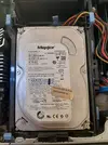
Tutti quelli che hai linkato sono 2.5 pollici
Io ho un DiamondMax 22 della maxtor 3.5 pollici
Posso montarlo senza problemk?
Ciao! Si lo puoi montare senza problemi, puoi metterci anche un adattatore se vuoi metterlo nello stesso slot! Verifica di avere l'attacco SATA però...!
riccarock
Utente Èlite
- 7,970
- 2,080
- CPU
- Amd Ryzen 3700x
- Dissipatore
- Noctua NH-D15
- Scheda Madre
- Asus Rog Strix X570 F-Gaming
- HDD
- Nvme WD SN850 Black 500Gb,Kingston Renegade 2TB,Toshiba P300 3Tb,WD Red Plus 4Tb,2 Toshiba MG08 16Tb
- RAM
- Corsair Vengeance 2x8Gb 3200Mhz Cl16
- GPU
- Asus Tuf OC 3060Ti
- Audio
- Edifier 1280DBs
- Monitor
- Asus Tuf Gaming VG279QM
- PSU
- Corsair RMX 750w Shift
- Case
- Fractal Design Define R6
- Periferiche
- Tastiera Custom
- Net
- Tim Fibra 1000
- OS
- Windows 10 Pro
Se la mobo è SATA 2 c'è l ha per forza
Si hai ragione.... svista mia, ho risposto velocemente e non mi ricordavo più che nelle specifiche c'era scritto SATA II , tant'è che glielo avevo anche detto nei post precedenti....?
Quindi senza Adattatore non posso usarlo?Se la mobo è SATA 2 c'è l ha per forza
Devi prendere gli adattatori
E butta via quel hdd già la marca è discutibile poi avrà minimo l.eta del pc
Inviato dal mio MI 9 utilizzando Tapatalk
Ci sono discussioni simili a riguardo, dai un'occhiata!
- Risposte
- 6
- Visualizzazioni
- 306
- Risposte
- 13
- Visualizzazioni
- 809
- Risposte
- 30
- Visualizzazioni
- 2K
- Risposte
- 9
- Visualizzazioni
- 444
- Domanda
- Risposte
- 3
- Visualizzazioni
- 420
Condividi:
Discord Ufficiale
Entra ora!
Discussioni Simili
-
 PROBLEMA SSD compatibilie con la mia scheda madre
- Iniziata da Klipy
- Risposte: 6
-
DOMANDA Consiglio acquisto SSD SATA 1 TB.
- Iniziata da Evos
- Risposte: 13
-
-
DOMANDA Seagate SkyHawk ST4000VX016 (4tb)
- Iniziata da fresco
- Risposte: 9
-
RISOLTO l' uso di un SSD tipo M.2 comporta la "perdita" di qualche porta SATA?
- Iniziata da pici_1251
- Risposte: 3